Electrode Fabrication on 2D Materials
Overview
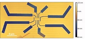
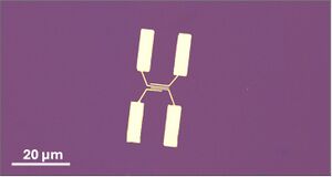
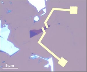
This process details the fabrication of electrodes on 2D materials like WSe₂ using the NanoFrazor system. The method combines NanoFrazor Thermal Scanning Probe Lithography (t-SPL) for high-resolution patterning (<2 µm) and laser lithography for larger features such as contact pads. This hybrid approach allows precise and efficient electrode fabrication, ensuring high-quality results.
Process Directions
Sample Preparation: To prepare the silicon substrate, start by cleaning the silicon wafer. Soak the wafer in acetone for ten minutes using a sonicator, followed by isopropanol (IPA) for another ten minutes, and finally DI water for the same duration. Once cleaned, dry the wafer thoroughly using nitrogen gas. Proceed by depositing a 3% PMMA-MA solution onto the cleaned wafer. Place the wafer at the center of the spin coater and spin coat it in two steps, first at 500 rpm for five seconds and then at 6000 rpm for sixty seconds. Bake the coated wafer at 165°C for ninety seconds on a hot plate. Next, deposit a 2% PPA solution on top of the PMMA-MA-coated wafer. Spin coat this layer in two steps, starting at 500 rpm for five seconds and then at 2500 rpm for one hundred and twenty seconds. Finally, bake the wafer at 110°C for one hundred and twenty seconds on a hot plate.
Nanolithography Using NanoFrazor (t-SPL): Begin the nanolithography process by configuring the NanoFrazor system. Prepare the tip by mounting it securely, referring to the "Tip Replacement" procedure if necessary. If required, burn the tip at 1150–1200°C (7.7 V) for thirty seconds. Calibrate the system by performing an IV curve check to ensure proper electrode connection. Position the sample using the focus motor and align the tip for pattern writing. Run the "Level Plane" function to align the stage relative to the tip. Set up the writing parameters by loading the pre-designed pattern file. Select the 2D patterning mode and adjust the depth to 100 nm. Configure the writer temperature between 850°C and 950°C to achieve the desired thickness, and enable Kalman mode with a gain of 0.2. Align the pattern using the session panel and ensure precision by activating "Active Field Stitching" and "Always Recalculate Sample Level Plane." Initiate the writing process and monitor its progress until completion.
Laser Lithography for Large Patterns: For creating larger features, such as contact pads, use a laser with a power intensity of 150 mW and set the exposure time to 70 microseconds.
Development: Immediately after completing lithography, develop the sample by submerging it in ethanol for 120 seconds. Rinse the developed sample with isopropanol to remove any residual ethanol and then dry it using nitrogen gas. Once dried, store the sample in a desiccator to preserve its condition until metal deposition.
Metal Deposition: Position the sample in an electron-beam evaporator or a similar system. Ensure a straight path for deposition by using a chip tray to hold the sample above the crucible. Begin by depositing a 15 nm layer of titanium at a rate of 0.2 Å/s, followed by a 35 nm layer of gold at 0.5 Å/s.
Lift-Off Process: To remove unwanted resist material, soak the sample in acetone for at least one hour or preferably overnight. Use a dropper to create bubbles and jets of acetone to dislodge large chunks of resist. For any stubborn residues, gently sonicate the sample at low power for one second. Afterward, rinse the sample thoroughly with ethanol and follow up with isopropanol. Dry the sample using nitrogen gas, then inspect it under a microscope to confirm the completion of the final electrode patterns.


