Robotic Stacker – WSe₂ Trilayer Gated Heterostructure
Jump to navigation
Jump to search
This recipe describes the MonArk NSF Quantum Foundry procedure for fabricating a WSe₂ trilayer gated heterostructure using the MonArk robotic stacking system. The process involves sequential pickup and deposition of five flakes (bold indicates gated layers)

Layers:
- Graphite (few-layer)
- hBN (15–18 nm)
- WSe₂ trilayer (contains occasional 4L, 5L+ regions)
- hBN (15–18 nm)
- Graphite (few-layer)
Stamp Preparation
- Use a PDMS-molded stamp fabricated with PC as the polymer (see “Figure 2”).
- Brass molds are employed to shape the PDMS tip, optimized for the MonArk stacker.
MonArk Stacker Axes & Control

- A: Vertical stage of stacking finger
- B: Goniometric tilt stage
- C: Rotation stage
- X/Y: Linear translation stages
- Z: Vertical stage for focus adjustment (20× or 50× objective)
- Resolution: 0.001 mm (linear), 0.0013° (angular)

Part 1 – Pickup of Flakes
Parameters:

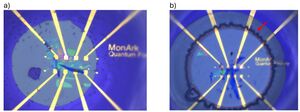
Figure 4. Stamp in contact with electrode substrate during final deposition. b) PC melting off the stamp with a circular front of PC collapsing toward center, denoted by red dotted circle. Notable feature is the finger-like channels indicated by the red arrow. Note image in b) is a different heterostructure.
- Polymer: Polycarbonate (PC) in chloroform
- PC concentration: 7% (w/v)
- Stage temperature: 150 °C
- Contact diameter: 100–200 µm
- Wait time in contact: 1–2 min
- Pickup speed: ~0.001 mm/s
- Total time per flake: 5–10 min
- Note: A PC concentration of 7% in chloroform was found to provide reliable pickup at 150 °C. Lower concentrations (e.g., ~6%) may require reduced pickup temperatures (~90–120 °C) but can lead to less consistent adhesion depending on flake thickness and stamp geometry.

Guidelines:
- Maximize overlap for gated flakes while ensuring electrode access.
- Rotate gated flakes to ~120° separation for three distinct electrodes.
- Position hBN layers to isolate gated flakes and avoid full coverage of subsequent layers.
Tips:
- Alternate between lowering and lifting the stacking finger to avoid sudden movements.
- Look for a grayish color change indicating successful adhesion to the stamp.
Part 2 – Deposition onto Substrate
Temperature range:
- PC flow temperature: 190 °C
- PC melt temperature: 225 °C
Procedure:
- Align stack so each graphite flake and the WSe₂ trilayer overlap independent electrodes.
- Slowly raise stacking finger in 0.001 mm steps while maintaining PC temperature between flow and melt points.
- Watch for “front” formation (PC detaching toward the stamp center) and finger-like melt channels.
- Continue until the PC fully detaches from the stamp without tearing the heterostructure.
Tips:
- Mold tips have higher curvature than double domes; avoid abrupt sliding at high temperatures.
- Adjust temperature dynamically during deposition to control PC flow rate (~2 °C/sec heating).
- When the contact front passes over the heterostructure, pause or slightly lower the stamp to prevent damage